(China (Mainland))

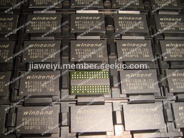
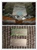
Product Summary
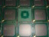
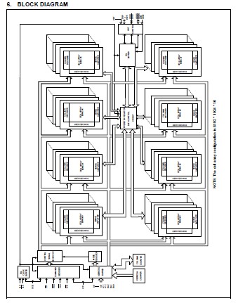
The W971GG6JB-25I is a 1G bits DDR2 SDRAM, organized as 8,388,608 words × 8 banks × 16 bits. This device achieves high speed transfer rates up to 1066Mb/sec/pin (DDR2-1066) for various applications. The W971GG6JB-25I is sorted into the following grade parts: -18, -25, 25L, 25I, 25A, 25K and -3. The -18 grade parts is compliant to the DDR2-1066 (6-6-6) specification. The -25/25L/25I/25A/25K grade parts are compliant to the DDR2-800 (5-5-5) specification. All I/Os of the W971GG6JB-25I are synchronized with a single ended DQS or differential DQS- DQS pair in a source synchronous fashion.
Parametrics
W971GG6JB-25I absolute maximum ratings: (1)Voltage on VDD pin relative to VSS VDD: -1.0 ~ 2.3 V; (2)Voltage on VDDQ pin relative to VSS VDDQ: -0.5 ~ 2.3 V; (3)Voltage on VDDL pin relative to VSS VDDL: -0.5 ~ 2.3 V; (4)Voltage on any pin relative to VSS VIN, VOUT: -0.5 ~ 2.3 V; (5)Storage Temperature TSTG: -55 ~ 150 ℃.
Features
W971GG6JB-25I features: (1)Power Supply: VDD, VDDQ = 1.8 V ± 0.1 V; (2)Double Data Rate architecture: two data transfers per clock cycle; (3)CAS Latency: 3, 4, 5, 6 and 7; (4)Burst Length: 4 and 8; (5)Bi-directional, differential data strobes (DQS and DQS ) are transmitted / received with data; (6)Edge-aligned with Read data and center-aligned with Write data; (7)DLL aligns DQ and DQS transitions with clock; (8)Differential clock inputs (CLK and CLK ); (9)Data masks (DM) for write data; (10)Commands entered on each positive CLK edge, data and data mask are referenced to both edges of DQS.
Diagrams
 |
 W971632AF |
Other |
|
Data Sheet |
Negotiable |
|
||||||||||||||||||||||
|
W971GG6JB25I |
|
IC DDR2 SDRAM 1GBIT 84WBGA |
Data Sheet |
|
|
||||||||||||||||||||||
|
W971GG8JB-25 |
|
IC DDR2 SDRAM 1GBIT 60WBGA |
Data Sheet |
|
|
||||||||||||||||||||||