(China (Mainland))


Product Summary
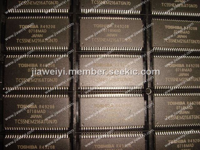
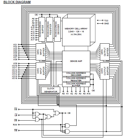
The TC55NEM216ATGN70 is a 4,194,304-bit static random access memory (SRAM) organized as 262,144 words by 16 bits. Fabricated using Toshiba’s CMOS Silicon gate process technology, the TC55NEM216ATGN70 operates from a single 5V ± 10% power supply. Advanced circuit technology provides both high speed and low power at an operating current of 3 mA/MHz (typ) and a minimum cycle time of 55 ns. The TC55NEM216ATGN70 is automatically placed in low-power mode at 1.8 μA standby current (typ) when chip enable (CE) is asserted high.
Parametrics
TC55NEM216ATGN70 absolute maxing ratings: (1)VDD Power Supply Voltage: -0.3~7.0 V; (2)VIN Input Voltage: -0.3~7.0 V; (3)VI/O Input/Output Voltage: -0.5~VDD + 0.5 V; (4)PD Power Dissipation: 0.6 W; (5)Tsolder Soldering Temperature (10s): 260 ℃; (6)Tstg Storage Temperature: -55~150 ℃; (7)Topr Operating Temperature: -40~85 ℃.
Features
TC55NEM216ATGN70 features: (1)Low-power dissipation Operating: 15 mW/MHz (typical); (2)Single power supply voltage of 5 V ± 10%; (3)Power down features using CE; (4)Data retention supply voltage of 2.0 to 5.5 V; (5)Direct TTL compatibility for all inputs and outputs; (6)Wide operating temperature range of -40℃ to 85℃; (7)Standby Current (maximum): 20 μA.
Diagrams
| Image | Part No | Mfg | Description |  |
Pricing (USD) |
Quantity | ||||
|---|---|---|---|---|---|---|---|---|---|---|
 |
 TC55NEM216ATGN70 |
Other |
|
Data Sheet |
Negotiable |
|
||||
|
TC55NEM216ATGN70LA |
Other |
|
Data Sheet |
Negotiable |
|
||||