(China (Mainland))

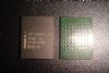
Product Summary
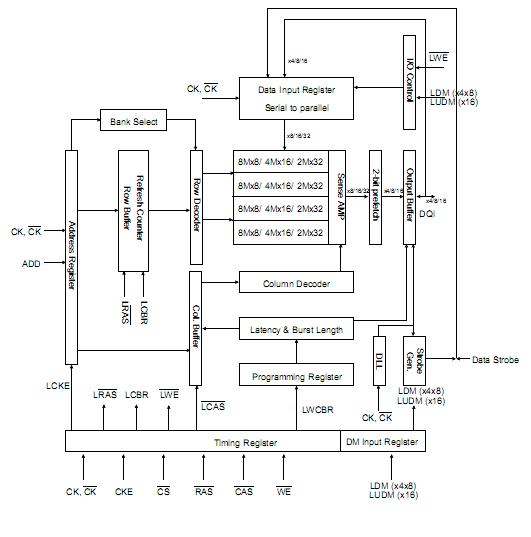
The K4H561638J-LCB3 is a double data rate synchronous DRAM organized as 4x 8,388,608 words by 8bits. It is fabricated with SAMSUNG’s high performance CMOS technology. Synchronous features with Data Strobe allow extremely high performance up to 400Mb/s per pin. I/O transactions are possible on both edges of DQS. Range of operating frequencies, programmable burst length and programmable latencies allow the K4H561638J-LCB3 to be useful for a variety of high performance memory system applications.
Parametrics
K4H561638J-LCB3 absolute maximum ratings: (1)Voltage on any pin relative to VSS:-0.5 to 3.6 V; (2)Voltage on VDD & VDDQ supply relative to VSS:-1.0 to 3.6 V; (3)Storage temperature:-55 to +150℃; (4)Power dissipation:1.5 W; (5)Short circuit current:50 mA.
Features
K4H561638J-LCB3 features: (1)All inputs except data & DM are sampled at the positive going edge of the system clock(CK); (2)Data I/O transactions on both edges of data strobe ; (3)Edge aligned data output, center aligned data input; (4)LDM,UDM for write masking only (x16); (5)DM for write masking only (x4, x8); (6)Auto & Self refresh; (7)7.8us refresh interval(8K/64ms refresh) ; (8)Maximum burst refresh cycle : 8; (9)66pin TSOP II Lead-Free & Halogen-Free package; (10)RoHS compliant; (11)Double-data-rate architecture; two data transfers per clock cycle; (12)Bidirectional data strobe [DQS] (x4,x8) & [L(U)DQS] (x16) ; (13)Four banks operation; (14)Differential clock inputs(CK and CK); (15)DLL aligns DQ and DQS transition with CK transition.
Diagrams
C/LA2") |
 K4H510438B-G(Z)C/LA2 |
Other |
|
Data Sheet |
Negotiable |
|
||||
|
K4H510438B-G(Z)C/LB0 |
Other |
|
Data Sheet |
Negotiable |
|
||||
|
K4H510438B-G(Z)C/LB3 |
Other |
|
Data Sheet |
Negotiable |
|
||||
|
K4H510438B-G(Z)C/LCC |
Other |
|
Data Sheet |
Negotiable |
|
||||
|
K4H510438C-UCA2 |
Other |
|
Data Sheet |
Negotiable |
|
||||
|
K4H510638E-LA2 |
Other |
|
Data Sheet |
Negotiable |
|
||||